CubicPV is narrowing down location search for 10-GW silicon wafer factory
There are multiple steps in the silicon solar panel manufacturing process: silicon is melted and shaped into ingots that are sliced into wafers, which then turn into cells that are finally assembled into a solar panel. The United States is trying to increase domestic manufacturing representation in each of these steps, but thus far, new factory announcements have largely been focused on final solar panel assembly. There are just a few cell factories planned and even fewer wafer or ingot setups.
Wafer manufacturing can be a very mechanical and specialized process. The entire wafer industry is primarily located in China today, where labor costs are low and technical know-how is hoarded. Qcells and its parent company Hanwha Solutions intend to start a 3.3-GW all-inclusive silicon solar panel manufacturing factory in Georgia — keeping the ingot, wafer and cell supply for Qcells solar panels.
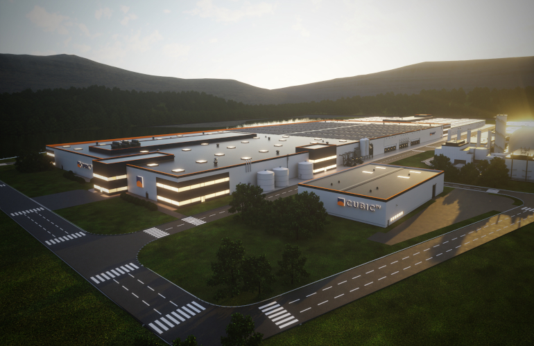
CubicPV is the only manufacturer focusing solely on domestic ingots and wafers on a large scale — the Massachusetts-based technology company plans to open a 10-GW ingot and wafer factory in the United States in 2025. CubicPV CEO Frank van Mierlo told Solar Power World that the company has narrowed down its location search for the 1.5 million-sq.-ft factory to two sites and expects to make a final decision this summer. There are many factors going into site selection, with labor force, electricity sources, water supply and limited seismic activity being the core priorities, he said.
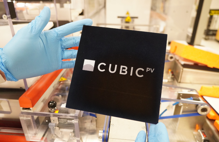
“I always joke that this must be the most boring product in the world. It’s a gray square made by a bunch of people who are pretty square themselves. It doesn’t get more boring, but, boy, is there a lot of detail,” van Mierlo said. “It’s very high-tech, there’s a ton of inputs and all this supply chain needs to be created and built.”
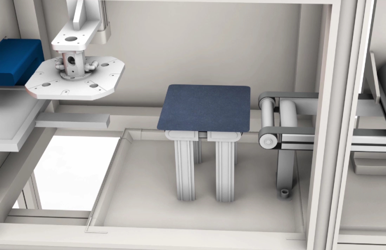
CubicPV will hire more than 1,000 workers to produce 1 billion wafers each year. Workers will push silicon into 600 furnaces every day to form ingots, before cooling and eventually moving them along to be thinly sliced into wafers.
Credit: CubicPV Vimeo
“There’s a lot of things that go into these factories. You need a swimming pool of water every hour [for heating and cooling], a lot of electricity. All of this is done in an argon-gas atmosphere. You need noble gases, you need to clean the water,” van Mierlo said. “You need a location that’s relatively free of any vibration. You can’t have a big highway with heavy trucks putting vibrations in the ground that can cause you to lose structure and destroy your production run.”
CubicPV formed in 2021 as a merger of 1366 Technologies and Hunt Perovskite Technologies, two U.S. solar R&D companies focused on wafers and perovskites. 1366 had a lengthy relationship with Hanwha Solutions in improving cell efficiencies on single-junction solar panels. CubicPV is invested in developing tandem PV designs and has a wafer and cell supply agreement with India’s Waaree.
Although CubicPV has championed a “direct wafer” technology that makes wafers directly from molten silicon, this initial 10-GW wafer factory will function in a more traditional sense making mono-wafers from ingots. The company is not abandoning its Direct Wafer development, and R&D continues, but in order to get wafer manufacturing set up in the United States now, CubicPV went the traditional route first.
“I want to build a factory that is as good as the best factories in China. That’s our starting point, then we’ll get better,” van Mierlo said. “You’ve got to recognize that China has invested $200 billion to get where they are today. The IRA is an even larger investment than what China made, and we’re going to do better.”
CubicPV will likely produce p-type and n-type M10 and G12 wafers for U.S. and international solar cell developers. A 10-GW wafer factory may seem ambitious, van Mierlo said, but the game has no other players.
“Today the U.S. market is about 50 GW [of annual installed capacity]; 10 GW is only 20% of market share, so it’s not that large in that scheme,” he said. “I think the U.S. market will grow to about 100 GW by the time this factory comes online. If you look at it compared to the size of the opportunity, it’s actually not that large.
“We’re really getting ready to do this. It’s a big deal because, today, 100% of wafers are being manufactured by China — 97% in China and the remaining 3% is Chinese companies inside Vietnam,” van Mierlo continued. “To diversify that supply chain is good for humanity.”
See our list of U.S. solar manufacturers here.